 | The JBL "Bass Wave" amplifier
The JBL "Bass Wave" amplifier is a small 100-watt amplifier with built-in active filter with a single-pole high-pass at 10 Hz combined with a single-pole lowpass at 85 Hz.. It costs an amazingly low $50 US. It also comes with line and speaker-level inputs and a volume control for level-matching, and an "auto signal sensing power switch". It also features reasonable build quality. However, it is not an "audiophile" or even hifi-quality amplifier - a few corners have been cut in the design in order to keep the price so low. However, it may be possible to improve it a bit with a few tweaks. So, what's "wrong"?
Ok, so what's wrong with the Basswave? Well, I've got some of the "faults" listed below: - The Bass Wave amplifier uses a "class-B" output stage. Most audio amplifiers use a "class-AB" output stage because class-B circuits are prone to crossover distortion, which audibly affects the output at low volumes. The notch distorion may show as a fuzziness or raspy character at very low levels. Note that this is of less consequence in a subwoofer design, as the effect is less noticeable at low frequencies, and how many times have you listened to a subwoofer at low volumes?
- The output devices in the Bass Wave amplifier are used in a common collector configuration. While this raises the voltage gain of the stages (and is a cheap way to save parts), it also raises the output impedance, which in turn reduces the current dumping and damping factor of the amplifier. The voltage gain should come from the driver stage of the amplifier, not the output devices. (Correction - Jason Cuadra says that it is a composite 2 stage common emitter with local feedback set by R31 and R30, setting gain to 10).
- There is no short-circuit protection in the output stage of the Bass Wave amplifier.
- Power output seems a bit low for a subwoofer amplifier.
The schematic for the Bass Wave amplifer is available at the following location: http://www.diysubwoofers.org/projects/other/basswave/BASSWAVE.pdf Bill Wilson of the DIY Loudspeakers List described the circuit design of the Bass Wave amplifier as follows in message to the List (which I've edited slightly here): " A low pass input network feeds the main amplifier which is a LF347 op amp driving a modified darlington current amplifer which is wired to also give voltage gain. The LF347 is a nice op amp with gain bandwidth product of 4 Mhz and FET inputs. There is no quiescent current biasing of the output transistors. The bases of the 1st stage output transistors (TIP31C and TIP32C) are copper bound to each other giving 1.2 volts of crossover distortion. There are no emitter resistors anywhere, not even in the 2nd stage TIP35C/TIP36C emitters. As far as driving 4 ohms go, the TIP35C/TIP36C transistors have the current rating to handle this but I don't know about the power supply. There are 4700uF capacitors filtering the rectified DC and I would want to load test the transformer before feeling safe about it. There is a thermistor on the heat sink wired to an op-amp comparator which will shut the amp down at some temperature, but note that there is no short circuit protection on the output transistors. There is an audio signal detection circuit that drives the front panel LED, but the power amp insided is not powered down, just the LED. " Modifications (proposed):
Listed below are some modifications to the amplifier that have been PROPOSED by members of the DIY Loudspeakers list. These modifications have not actually been tried out, but they do sound good enough for consideration: - Jason Cuadra: " To increase output current capability, double up the filter caps, change to beefier rectifiers. ( a la 5A 200V ) and double the output transistors(in parallel), but with an emitter resistor for each one of about 0.1 ohm, to make them share current. To bias it into class AB would require re-designing the whole stage: - It would require an additional 2 power resistors, 2 smaller resistors, 2 constant current sources each made of 2 transistors and a resistor, and a VBE multiplier stage made of a transistors and 2 resistors; reducing the gain of the output stage (from 10 to 3 or 4), and re-checking the feedback loop stability. "
This is a circuit showing some of the some mods I talked about, with the addition of current limiting / short cct protection, and this is another circuit showing the actual modifications to be made to the amplifier. Warning, the short circuit protection scheme is untested. It may oscillate during over current conditions or may not be set to a low enough current to protect the output devices. For short circuit protection, emitter resistors ought to be more like 0.15 ohms each. Current limit in each output device will be set to 0.7V / 0.15 ohms, or about 5A each. Additional transsistors to do the current limiting can be TIP31A and TIP32A like the driver transistors.
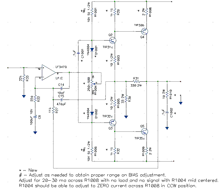
- Richard Hall: (see diagram of modified circuit for reference) " This is just a change of the design as I would start IF I owned one. The resistor valuse are pure guesstimations. As I have no data books on hand and do not have one of these amps, I can only pick values from other similar designs. But the point being that this approach should fix the lack of proper biasing on the amp. Also there is an additonal supression network on the output to keep things from oscillating in the event that the amp should show any sign of instability. R1003/R1005 give a little bit of stability to the drivers by inducing a small amount of feedback into the stage and help to stabilize the biasing. The diodes should be insulated and mounted on the heatsink. I place heatshrink tube on the leads, dip them in epoxy to cover the diode and the leads at the body and them let it set until soft and moldable, then stick them to the heatsink to form a flat spot on them for better heat transfer. When the epoxy has setup hard, I put some Wakefield compound on the flatside and then clamp them down with a small spring clip. The bias pot should be adjusted in the center and should get about 20-30 ma. across R1008. The value of the pot should work out to something in the 250-500 ohm range... maybe as low as 100 ohm. If the fine adjustment is not needed/wanted, then leave the pot out, in which case the final current gain to the drivers is set by the R1001/R1006 pair. As I do not know what type of current gain is needed in these stages/transistors, these values may be off by a fair margin. I would not play with this without a variac or adjustable power supply to bring the amp up slowly to monitor the output current. If someone has balls, (grin), they may want to just use some small value fuses... like 1 Amp. The circuit changes should be fine. Again the final value of the bias pot and the resistors R1001/R1006 are total a guess. But with some experimenting the correct values should be fairly easy to figure "
|
|